Subtotal: $110.00

Intrinsicly evisculate emerging cutting edge scenarios redefine future-proof e-markets demand line


Green Nanotechnology is a transformative force across multiple scientific, industrial, and healthcare domains, enabling precision engineering at the atomic and molecular levels. The following futuristic research fields are poised to revolutionize technology, industry, and universal well-being. Kadamba can develop relevant green nanoparticles to support and accelerate your pioneering research.
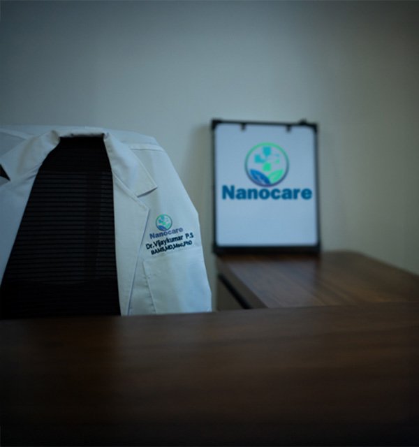
Nano Care, a pioneering service initiative and global venture by Kadamba, is transforming wellness through patented green nanotechnology, advanced analytics, and bio-signal monitoring. Dedicated to personalized, preventive, and real-time health solutions, Nano Care ensures unmatched efficacy and safety for long-term well-being. Its chemical-free formulations guarantee zero side effects, setting a new standard in holistic healthcare with eco-friendly nano-pharmaceuticals and precision-targeted interventions. Nano Care is more than a venture-it's a commitment to a healthier, sustainable future for humanity.


.jpg)